Active smart label with kinematic MEMS sensors
One example for the growing requirement of system integration is the development and fabrication of RFID labels. One decade ago the labels consisted of paper and had been used as info carrier to deliver visual and machine readable information. Some years later the paper label was replaced by passive RFID (radio frequency identification) labels with an integrated bi-stable display to show the necessary information like distributor, time and tracking code as well as other important transport information. |
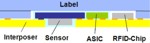 Figure 1: Packaging solution for RFID label with integrated sensor functions for shock, inclination and temperature |
The latest trends focus on RFID labels with integrated sensor functions. One example is an active radio frequency identification label for the monitoring of shock, inclination and temperature during transportation processes. This label consists of a polymer substrate, a RF-chip with antenna, a battery for power supply and a sensor system consisting of a micromechanical transducer and the signal processing electronics. All these elements have to be integrated on the thin label substrate fulfilling specific requirements for the sensor system like low power consumption, high signal to noise ratio, high temperature stability and low device/sensor thickness. A packaging solution of such a label is presented in top right figure. |

|
To integrate all the elements into one label a flexible printed board (250 µm thick PET) is used as interposer which carries the sensor, the sensor ASIC and the RFID ASIC. The bottom right picture shows the interposer after its fabrication with conductive pathways and mounted chips. This interposer can be fabricated and tested independently from the label production and assembly and has the special feature of integration ability of further sensor functions. The currently used acceleration sensor provides information about shock and inclination and is covered by a 200 µm thick silicon cap. This leads to a relative thick sensor stack of about 450 µm by using a 250 µm thick sensor substrate.
The capped sensor can only be integrated into the label by punching a window into the interposer substrate material. After that it is mounted face down on the interposer substrate. Future interposer versions will be equipped with sensors which are capped by thin film packaging using a thin layer stack of oxide and nitride to protect the active part of the sensor. This free-standing sensor capping membrane is fabricated by means of etching of a sacrifical layer underneath the membrane.
The developments were carried out in cooperation with KSW Microtec AG (Dresden), ELMOS AG (Dortmund) and Schenker AG (Dresden) within the research project ASIL.
Contact
Dr. Danny Reuter
E-Mail:
danny.reuter@…