Research Topics
Network models for graphene nanolaminates as electrical conductors
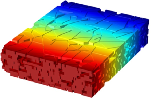
Graphene nano-laminates (GNL) consist of disordered stacked sheets of pure graphene, which form a macroscopic material. They are fabricated from suspensions of graphene or graphene oxide. GNLs can be prepared as films or can be spun into fibers. The material is flexible, strong, and lightweight. After reduction, doping and thermal treatment GNLs can reach very high electrical conductivities of several tens of MS/m. Thus, they have the potential to be a lightweight alternative to metals in many application fields....
The results of our simulations show clearly, that out-of-plane conductivity and flake size are the key factors to reach a highly conductive macroscopic material [2]. Only for GNLs consisting of large flakes of several tens of microns and good out-of-plane conductivities, we can transfer the excellent conductivity of the single graphene flakes to the macroscopic conductivity.
In order to check our models, GNL-films consisting of size selected graphene flakes have been prepared and analyzed carefully [3]. As simulation and experiments are in a perfect agreement, we conclude that our microstructural model is valid and provides a solid basis for a systematic optimization of graphene nano-laminates towards metallic conductivity.

Schematic view of our GNL-model
Further reading:
- L. Rizzi, J. Schuster, S.E. Schulz et al.; Computationally efficient simulation method for conductivity modeling of 2D-based conductors, Comp. Mat. Science, 2020
- L. Rizzi, J. Schuster, S.E. Schulz et al.; Electrical conductivity modeling of graphene-based conductor materials, ACS appl. materials & interfaces, 2018
- L. Rizzi, J. Schuster, S.E. Schulz et al.; Quantifying the influence of graphene film nanostructure on the macroscopic electrical conductivity, Nano Express, 2020
Simulation Models Related to Silicon Nanowire Field-Effect Transistors
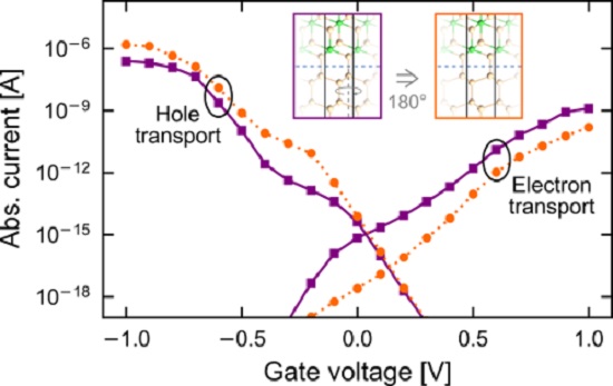
Silicon nanowire based field-effect transistors offer a promising and reliable way to improve the performance of circuits. In combination with suitable contacts, reconfigurable transistors can be fabricated, which allows for more flexible circuit design.
Simulations were performed to study surface and quantum effects, which become increasingly relevant for nanowires with small diameters. The local states in Fig. 1 shows how the band gap increases towards the surface of the nanowires. Similarly, the band gap increases when the nanowire diameter is decreased [1]....
Fig. 1: Radially resolved local density of states for two different silicon nanowires

Fig. 2: Transfer characteristic of a silicon-based reconfigurable field-effect transistor with NiSi2 contacts
Further reading:
- F. Fuchs, S. Gemming, J. Schuster; Radially resolved electronic structure and charge carrier transport in silicon nanowires, Physica E Low Dimens. Syst. Nanostruct., 2019
- F. Fuchs, S. Gemming, J. Schuster; Electron transport through NiSi2-Si contacts and their role in reconfigurable field-effect transistors, J. Phys. Condens. Matter, 2019
- M. B. Khan et al.; Towards Reconfigurable Electronics: Silicidation of Top-Down Fabricated Silicon Nanowires, Appl. Sci., 2019
- F. Fuchs et al.; Formation and crystallographic orientation of NiSi2-Si interfaces, J. Appl. Phys, 2020
Quantum chemical simulation of atomic layer processing
Atomic layer deposition (ALD) is a thin-film deposition technique based on sequential, self-limiting reactions between gaseous precursors and functional groups on the surface. ALD enables atomic level control of film thickness, which is indispensable for advanced nanofabrication. By means of quantum chemical calculations we have studied the ALD of metallic Cu using the Cu(acac)2 precursor [1-2]. In the first half-cycle of Cu ALD, a sequential dissociation and reduction of the Cu precursor [Cu(acac)2 → Cu(acac) → Cu] are observed (see Fig.1). In the second half-cycle, H atoms easily lead to the bond breaking of ligands, and thus release the surface species into the gas-phase [3]....
_surface_logo.jpg)
Fig. 1. Reaction pathways for the dissociation of Cu(acac)2 on the Ta(110) surface.
- X. Hu, J. Schuster, S. E. Schulz, T. Gessner; Surface chemistry of copper metal and copper oxide atomic layer deposition from copper (ii) acetylacetonate: a combined first-principles and reactive molecular dynamics study. Phys. Chem. Chem. Phys., 2015.
- X. Hu, J. Schuster, S. E. Schulz, T. Gessner; Simulation of ALD chemistry of (nBu3P)2Cu(acac) and Cu(acac)2 precursors on Ta (110) surface. Microelectronic Engineering, 2015.
- X. Hu, J. Schuster, S. E. Schulz; Multiparameter and parallel optimization of ReaxFF reactive force field for modeling the atomic layer deposition of copper. J. Phys. Chem. C, 2017.


