Projects
Second project period
The research program comprises 8 projects:
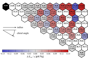
DFT calculations of the change of the CNTs band gap upon axial strain, drawn in the CNT periodic table. Dark colors = strong response. Red/blue = Band gap opening/closing.
The focus of the project is primarily the application ab-initio results of the first project phase to support development, technology and the design of nano scale devices integrated into micro scale sensor structures. At the same time, atomistic simulation models are going to be further developed with respect to their abilities such that more realistic models emerge. This simulation concept along two different lines – the combination of ab-initio models with effective device models – shall be further pursued. In detail, the following goals arise from these objectives:
- Simulation of electronic properties of carbon nanotubes (CNTs) within realistic sensor structures with particular reference to static and dynamic, electrical fields
- Further development of the models for optical properties of strained CNTs, modeling approaches for local analytics together with TP4.
- Further development of the multi-scale simulation infrastructure for the optimization of the sensor design with regard to effects on the nano scale, together with TP2 and TP6
Partners
Prof. Thomas Geßner,Prof. Michael Schreiber
The subproject (TP) 2 deals with the methods and software development for the high order multilevel and multidomain compact NEMS-models for system design and simulation together with external electronics.
The main focus lies on a general method for the modeling of nano structures within micro structures whereas data from atomistic simulations are linked to FE-simulations of the micro structure. Furthermore, project support FE simulations in TP3, 4, 5 and 7 and collaborate with TP3, 5 and 7 in N/MEMS design and characterization.
The working packages are dealing with methodic and algorithmic tasks to support N/MEMS model development. For this purpose, behavioral equations of micro- and nano components shall be formulated. Information of the nanocomponents are going to be parameterized by TP1 on the basis of ab initio atomistic simulations. In parallel, complex form- and functional MEMS elements are going to be calculated by FEM-simulations.
Possible parameter variations within N/MEMS should be adapted to analogous components. For the development of evaluation circuits and the firmware of the sensor, system models are strongly required. Based on the generic CNT models from the first project phase, adoptions to distinct device designs are planned within these models.
In cooperation with TP3 and TP5, a MEMS test platform is being developed. It combines a movable platform for SWCNTs, sensors, thermal actuator, electrostatic sensors for the displacement measurements, piezoresistive sensors for force-measurements and a pointer in order to amplify movements for optical displacement measurements. The test platform shall be customized to different tasks: static and dynamic analysis of SWCNTs, reliability and fatigue of several types of different nanomaterials (CNTs, nanowires, nanomembranes etc.). The sensor prototypes being prepared within the first project phase are far away from the ideal and periodic models of CNTs (TP1). Therefore, in the second phase, system (TP2) and reliability (TP3) models should be improved and adapted to the measurement results. These adaptations will be based on the data obtained on the atomic scale by AFM, REM and TERS (TP4) depending on parameter variations of technological processes like DRIE and DLP (TP5).
Furthermore, the methods for the gap reduction between the electrodes proved in the first funding period shall be used for the fabrication of different capacitive sensor prototypes being designed for various frequency ranges condition monitoring sensors.
To integrate the CNT technology into systems the subproject deals with two topics: Further introduction of nanoscale parameters in the specification and verification process and development of high-sensitive electronics to amplify the sensing signal. The specification and verification of NEMS requires the introduction of parameter variations in the system models and in the verification process. Especially in analog domain such variations shall be checked using new monitoring features within the simulation runs and also within the hardware. Furthermore these volatile parameters lead to adaptive supply and measurement circuits to make the sensor signal usable with standard digital hardware.
Partners
Prof. Jan Mehner,Prof. Ulrich Heinkel
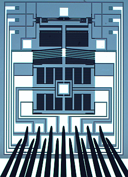
Tensile testing platform for nano-functional elements featuring a thermal actuator, displacement and force sensor following a "sample centric approach". Overall size of the device: 4.7x3.7mm
The objective of TP3 during the second phase of the project is the design, technology development and realization as well as the characterization of a technology-neutral, universal and highly miniaturized fatigue test platform in MEMS technology. This platform will serve for the systematic thermo-mechanical loading of bottom-up heterogeneously integrated nano-functional elements under realistic loads, including the effects of pressure, temperature and humidity. On the MEMS scale, this represents a completely new approach. First, the focus is on DEP self-assembled and micro-positioned CNTs, later other nanowires or nano membrane structures manufactured from Si, BN or Al are of interest. The second phase is consistently aiming at the newly emerging challenges of reliability assessment at the nano scale. To reach this goal, the cooperation with the TP 1, 2, 4, 5, 6 and 8 is mandatory.
The first step includes the design for the development of the fatigue testing platform as well as the apparatus of the simulative and experimental methods for reliability assessment. The aim is the consistent integration and purely electrical control and readout of the individual MEMS components into a dynamic mechanical testing device which is capable of applying alternating and subcritical loads. Very important is the involvement of the other TP regarding technological integration, especially regarding the compatibility of the targeted nano-functional elements of the platform, combined with maximum universality of the testing platform itself. Key philosophy here is the "sample centric approach": The testing device may be build, if necessary, as a result of the MEMS processes, around the already assembled test specimen.
Step two bundles in cooperation with TP2, the development of design concepts, the optimization using FE simulation, used for the layout of the MEMS platform, and the integration of multi-scale models of molecular dynamics (TP1) into the design environment foreseen for fatigue analysis and description of failure mechanisms.
Step three involves the development of technologies for the fatigue testing platform, the integration of the MEMS components and the testing of integrated nano-functional elements, provided by TP5, 6 and 8.
The final step aims at the experimental validation of the fatigue testing platform and the thermo-mechanical characterization of nano-functional elements compared to the simulations.
Partners
Prof. Bernhard Wunderle,Prof. Karla Hiller
The effects confined down to low dimensional scales will always be present and strongly define the overall micro/nano system device performance. Understanding these effects on the nanometer scale will allow us to successfully reach the goals of the project in the second phase.
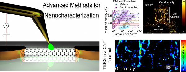
As exemplified in the first funding period, our extended techniques are able to address the corresponding nanoscale regime. Nevertheless, for several extreme cases the spatial resolution currently attainable and therefore the information spectrum are not high enough. In this regard, extending even further our methods towards complementary techniques becomes a critical goal worth pursuing. To this end we propose to add scanning tunnelling microscopy (STM) and µ-ellipsometry spectroscopy to the toolbox of nanoscale characterization methods in TP4.
Given the experience of Prof. Zahn group in optical spectroscopy, we propose to apply spectroscopic µ-ellipsometry in order to obtain the optical response of different CNT, rolled-ups, and silicon devices in collaboration with TP6, TP7, and TP8. The modelling and interpretation of the ellipsometer data will be performed in collaboration with calculations from TP1 in order to obtain the electronic transition energies that can be directly correlated with CNT chirality.
The extension to STM studies builds on the remarkable experience in the group of Prof. Hietschold in STM characterization of organic nanomaterials and metal/organic interfaces. In addition to all the foregoing, the consolidation of tip-enhanced Raman spectroscopy and related techniques will be a focus point in TP4.
Recently, other groups illustrating the unique potential of TERS in CNT research achieved impressive results at the single carbon nanotube level. However, the reproducibility of TERS results is an issue that compromises the widespread application of TERS; in the next phase we will tackle this issue down. Building on the rich experience obtained during the first funding period, we are well in the way to push the limits of TERS in terms of reproducibility. It will be investigated the role of several parameters such as environmental effects and tip properties on the electric field enhancement in TERS experiments and simulations with TP3. This goal will be pursued experimentally by optimizing the tip fabrication process and mechanical stability of our setup, as well as computationally, by improving the FEM simulation tools developed in close collaboration with TP2. The stress characterization of sensors and actuators will be a strong collaboration point with TP2 and TP3 using Raman spectroscopy, and also assessing Kelvin probe force microscopy for strain characterization. We will continue our work with TP5 in order to investigate the CNT-Au nanoparticle interaction towards the development of an optical plasmon-based sensor and extend further exciting developments obtained in the first funding period.
Partners
Prof. Michael Hietschold,Prof. Dietrich R. T. Zahn
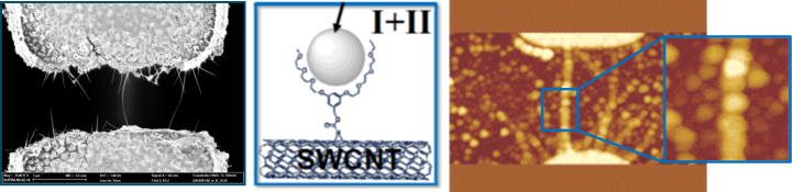
Carbon nanotubes (CNTs) integrated in microstuctures. Left: CNT contacted in a metal-coated Si-microstructure. Middle: CNT functionalization scheme. Right: AFM picture of CNTs functionalized with gold nanoparticles.
The elevation of this subproject is to transfer the knowledge of CNT integration and CNT-metal contact formation and the functionalization of CNTs with metal nanoparticles towards optical sensors. The motivation for the optical sensing is that the threshold voltage and the availability of charge carriers in the transistor channel on photoinduced excited surface plasmons (z. B. by applied metal nanoparticles) can be significantly altered in a CNT field effect-transistor (CNT-FET). Here, the optical characteristics (absorption cross section, refractive index) of the CNTs depend on the relative orientation of the CNT from the polarization direction of the incident light. Photodetectors based on CNT-FETs are known to possess low dark currents (Idark ⟨ 10-11 A) and low noise level (Iphot / Idark ⟨ 105) known to potential sizes of only a few square micrometers.
Scientific and technical basis of our approach is the planned usage of aspherical-elongated metal nanoparticles. The aim is to build a CNT functionalization framework of selective kind and controllable density. For this purpose, chemical and physical methods are first evaluated in the laboratory, in collaboration with Project 4; before the most promising method is implemented in the micro-technological environment. Afterwards, the manufactured components are optically and electronically characterized.
The work on the piezoresistive sensor in cooperation with the projects 2 and 3 will be continued in parallel, and lead to a fatigue test platform for nanomaterials.
Partners
Prof. Stefan E. Schulz,Prof. Heinrich Lang,
Prof. Thomas Otto
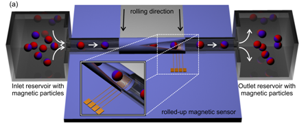
This magnetoresistve analyzer is a result of the first project period and has been published by G. Lin et al. in Nature Scientific Reports.
The project aims at developing micro- and nano-scale tubular magnetic field sensors by rolling magnetic nano-membranes, which detects small magnetic fields in a medium flowing through the tube and can be integrated with other sensor elements on the same tube section.
Fundamental theoretical and experimental studies are planned to elucidate the microscopic coupling phenomena in the geometrically induced giant magnetoresistance effect (GMR), which is the basic measuring principle of the sensor. For further optimizing the sensor function, deviations from the domain structure and the resonant modes of the planar initial film caused by the rolling up will be determined. For that purpose the magnetization of the ferromagnetic layer will locally be modified by ion irradiation such that magnetic segments of different spatial arrangement are defined along the tube. A systematic variation of the dimensions of the tube will allow to analyzing the geometric effects of rolling on the GMR effect. The proposed development of the soft X-ray tomography technique offers a worldwide unique access to three-dimensional detection of complex vector fields as the ones encountered in magnetism and magnetic detection.
Secondly, it is also an ideal starting point for a scale-adapted modeling, which embeds the magnetic functionality of complex-shaped detector geometries into classical device simulation. Finally, the joint expertise gained during the first phase of the research group within of the subprojects TP6 and TP8 will be exploited to prepare a multifunctional rolled-up element, which combines optical and magnetic detection capabilities and poses the very first attempt towards "lab-in-a-tube" concept.
Partners
Prof. Sibylle Gemming,Prof. Oliver G. Schmidt
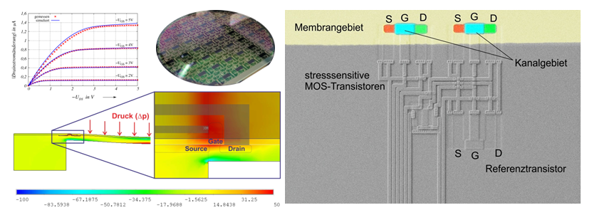
Left: Simulation and measurements of a silicon membrane / a mos sensor, photo of a processed wafer with testing structures; Right: Photo of a transistor bridge
The scientific investigations in TP7 – MOS detection for nano resonators – are based on the problem of decreasing sensor signals in micro and nano electromechanical systems due to the further downsizing of the mechanical sensor elements. For the conditioning of the sensor signals a concurrent reduction of noise is obligatory. Parasitic influences of connecting lines, bond pads and other packaging issues, which are a big part of the overall noise, can be strongly reduced by a tight coupling between transducer element and electronics.
Based on this assumption in this project the technological process steps as well as the device physics and the circuit technology will be investigated for the on chip integration of mechanical sensing elements and primary electronics in stress sensitive MOS transistors. Therefore pressure membranes, which are inducing mechanical stress inside the channel of transistors, are realized. The stress dependent variation of the charge carrier mobility in the channel of the MOSFET and the hereby influenced transistor parameters will be measured. Furthermore the piezo coefficients and the influence of the channel length and width on the sensitivity will be determined. Simulations with TCAD will be done to investigate useful physical effects for improving the stress detection. Another important point is to investigate the applicability of the piezo resistive effect on other sensor applications like acceleration and vibration sensors. The goal of the project is to prove the coupling of the mechanical with the electrical domain with small parasitic influences.
Partners
Prof. John Thomas Horstmann,Prof. Thomas Geßner
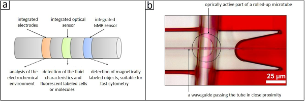
Fig: (a) Schematic drawing of a multi-functional rolled-up nanomembrane. The tube offers three different sensor functionalities (electrical, optical and magnetic) for the simultaneous detection of different properties of an analyte. (b) Optical wave guide to stimulate and analyze different modes. (Published by S. Böttner et al. in Applied Physics Letters)
Freestanding Nanomembranes represent novel structures with unique properties. In this project the sensoric capabilities of the nano-membranes are now expanded from the previous project and linked to actoric functions. By linking sensoric and actuatoric functionality with integrable three-dimensional nano-membranes, a new class of smart and, in consequence, intelligently acting assembled nanostructures arises.
Partners
Prof. Oliver G. Schmidt,Prof. Thomas Otto
First project period
The research program comprises 8 projects:
The aim of project 1 is the development of quantum mechanical simulation models in order to describe functional elements on the nanoscale as so-called nanomodels. These models will be coupled to commercial device simulations that rely on continuum models as well as the framework of continuum models developed in project 2. Besides the examination of efficient quantum mechanical simulation concepts for modeling of transport-properties and excited states of coated and doped CNTs, the development of standardized of these calculations shall be introduced into device-simulations in a parameterized way and furthermore, the description of the whole device system on a higher level is made possible, building up a complete hierarchy of simulations, starting from the nano scale and ending up in the complete device. The last point will be done in cooperation with the project 2.
Quantum mechanical ab initio simulations within the framework of time-dependent density functional theory (TDDFT) shall contribute to the analysis and optimization of already known sensors, but it shall also contribute to novel functional concepts relying on quantum-mechanical effects. There is a special interest in the dependency of the sensor-properties developed in project 5 on the fabrication parameters in order to influence those properties in a desired way.
Partners
Prof. Thomas Geßner,Prof. Michael Schreiber
Main research topics are the development of methods and tools for modeling multiphysical effects for micro and nano systems and the development of algorithms for the FE-model reduction (reduced order modeling) on sensor and system level. Coupling-effects and cross-effects in all physical domains (mechanical, thermal, electrical, fluid) as well as interactions with nanostructures have to be considered and they have to be efficiently and accurately implemented. Several system description languages such as SystemC-AMS must be assessed in this context. The system description languages have to be extended to support parameter variations at run time. The developed methods and tools are verified at different samples which utilize the nano effects and the nano scaled functional elements.
Partners
Prof. Jan Mehner,Prof. Ulrich Heinkel
Micro and nano sensors and systems are much more challenging than electronic systems regarding their valuation of thermo mechanical reliability and lifetime prediction. Within project 3 we will investigate mechanisms of fatigue, ageing and defects, as the amount, distribution and interaction of these effects is unknown so far. Novel experimental and theoretical methods (simulations) will be used and combined in order to discover and describe the behavior of the materials and defect mechanisms of the micro and nano components. As a result, new design rules and concepts for reliability valuation can be deduced. A main part will be the generation of test structures (coming from the different projects) for systematic manipulation of the nano structures, which allow dedicated induction of the ageing effects and failure mechanisms. New methods of thermo mechanical material characterization based on MEMS actuators will be developed and will provide the material characteristics as a function of relevant parameters such as temperature, humidity and vibration.
Partners
Prof. Bernhard Wunderle,Prof. Karla Hiller
Driven by the current downscaling tendency, analytical methods able to access as many as possible material properties within the nanometer scale, are of crucial importance for deeply ongoing basic studies and diverse applications. Based on the extended experience of the applicants in the area of Raman spectroscopy and scanning probe techniques, a Raman spectroscopy setup operable with nanometer spatial resolution will be developed. Additionally, different methods for electrical characterization at the sample surface (c-AFM, EFM/KPFM) will be used complementary for advanced surface analytics. Possible physics or technical related challenges like for example the establishment and the best usage of a sufficient field-enhancement for the tip-enhanced Raman effect (TERS), the tip and tip-sample contact optimization as well as questions related to the results interpretation, will be addressed. In time, with increasing experience and competence, applicable aspects will become of interest and will be handled in cooperation with the other groups of the overall project.
Partners
Prof. Michael Hietschold,Prof. Dietrich R. T. Zahn
Subproject 5 is targeted on the establishment of technological basics for the integration of carbon nanotubes (CNT) in MEMS/NEMS. Therefore the CVD (Chemical Vapor Deposition) method as well as the DEP (Dielectrophoresis) process will be deployed, whereby especially integrative aspects like scalability and reproducibility will be emphasized. Focal point is the specific placement and orientation of semi-conductive CNTs in special test and sensor structures. Thereby vital technological challenges like type selectivity, bonding, and complete integration at wafer level will be addressed. Progressive simulation and also in-situ methods will be applied for the development of the process. The functionalization of CNTs for the modification and extension of the sensor behavior is another main point. New precursors for the production of metallic and semi-conductive functionalizations will be developed and characterized. Processes like ALD (Atomic Layer Deposition) will be applied for their deposition.
Partners
Prof. Stefan E. Schulz,Prof. Heinrich Lang
Aim of the project is to investigate fundamental properties of novel geometric architectures consisting of assemblies of nanoparticles combined with rolled-up thin film systems that have magnetic functional layers. These nanoarchitectures will be fabricated in a way to reveal well defined magnetic transitions in response to an external magnetic field. In this respect, the magnetic state of the deposited films can be tuned by changing the number of magnetically-exchanged decoupled layers (Multilevel-System approach). The strong emphasis of the project is to make the fabrication process reproducible, thus opening the door to the commercialization of fabricated prototypes of magnetic sensor devices for on-chip applications.
Partners
Prof. Manfred Albrecht,Prof. Oliver G. Schmidt
Partners
Prof. John Thomas Horstmann,Prof. Thomas Geßner
Partial project 8 combines three research topics: micro-/nanofluidics, optical sensors for chemical and biological applications as well as novel rolled-up technology. This rolled-up technology will be applied to fabricate optofluidic sensor elements which can be easily integrated on-chip. Each of the sensor elements consist of a thin film which rolls-up, using targeted etching, into a tubular geometry due to a built-in strain gradient. The rolled-up tubes will act as optical ring resonators; they will be filled with liquid and, if necessary, will be emptied again. Changes in the index of refraction coefficient can be precisely measured by monitoring the shift of the optical modes arising in the resonator. The possibility of functionalizing the surface of the resonator before the roll-up process (via deposition of thin films of various materials, material combinations and molecules) opens a wide spectrum of applications. This includes the novel concept of hyperlensing or highly sensitive metamaterial fiber optics. An array of optofluidic rolled-up sensors can be prepared in a single fabrication process on-chip, which enables the possibility of an efficient parallel analysis of individual living cells.
Partners
Prof. Oliver G. Schmidt,Prof. Thomas Otto