Photovoltaics - silicon solar cells R&D
Based on the technological processes and the equipment available, the Center for Microtechnologies is able to contribute in photovoltaics R&D in several ways. The experience in thin film deposition, annealing, dry etching and film characterization represents the best prerequisite for research in process development. Most effort has been spent up to now in multi-crystalline silicon (mc-Si) cells which are usually applied within the large-scale photovoltaic power plants existing world-wide. Nevertheless, a large variety of processes is available for alternative cell concepts too.
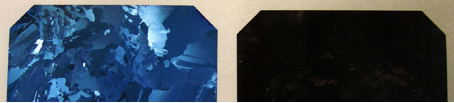
Since several years the Center for Microtechnologies and its industrial partners have been searching for processes offering high cell efficiency at reasonable costs. Due to the large experience in reactive plasma etching, the R&D activities were starting in the field of dry and maskless wafer texturing. Following the idea to reduce losses caused by light reflection at the cell surface, a well-defined "surface roughness" is aimed at. As sown in the Fig. below, the mc-Si wafer on the right appears black as a result of our dry texturing process. It corresponds to a solar weighted reflectance of about 1%.
Further work is going on with respect to the replacement of wet etch processes by dry etching: PSG removal, cleaning steps, back side emitter removal and saw damage removal. The fundamental character of this research at the ZfM allows for new approaches which have not been shown by others. According to the strong collaboration with Fraunhofer ENAS, these results are the base for further process development done by ENAS as research for industry.