At the Glance
The International Research Training Group (IRTG), which is funded by the German Research Foundation (DFG) of the Federal
Republic of Germany and the Ministry of Education (MoE) of the People's Republic of China, treats the more and more tremendous
challenges occurring with the progressive scaling of microelectronic device dimensions. Simultaneously, it addresses the demands
for more functionality of deep submicron and nanoscaled interconnect systems for future integrated circuits. New materials and
innovative concepts for their fabrication and characterization are required. However, to understand the properties and behavior
of materials on the nanoscale, extensive research is required.
The consortium of the International Research Training Group "Materials and Concepts for Advanced Interconnects" has long-time
experience in the field of microelectronics. With the outstanding scientific reputation of the partners, it is well prepared to
conduct the research and study program of the IRTG.
A research program featuring both applied and fundamental aspects will be established to treat mid- and long-term issues of
microelectronics metallization. Atomic layer deposition (ALD) of metals, new precursors for metal-organic chemical vapor deposition
(MOCVD), ultra low-k dielectrics and their mechanical and optical characterization together with inspection techniques on the
nanoscale will be considered. New and innovative concepts for future microelectronics, such as carbon nanotube interconnects or
molecular electronics along with silicides to form links to front-end of line processes, are of interest, as well as the evaluation
of manufacturing-worthy advanced materials. Moreover, the research program will address reliability and packaging issues of micro
devices. Highlighting links between fundamental materials properties, their characteristics on the nanoscale, technological aspects
of materials and their applications to microelectronic devices is the main objective of the program.
The different individual backgrounds of the project partners, bringing together electrical and microelectronics engineers,
materials scientists, physicists and chemists, will lead to multidisciplinary interaction. Consequently, synergy effects can be
expected in all fields of the research program. Considering that the projects combine fundamental research with applied aspects,
the envisaged IRTG provides a comprehensive program of materials science for mi-croelectronics. For the PhD students this will lead
to comprehensive knowledge in the field and ultimately to excellent job opportunities both in industry and academia.
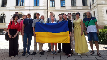
To provide comprehensive knowledge in the field of microelectronics and to educate the PhD students further, the specially tailored study program represents a fundamental part of the International Research Training Group. Lectures, seminars and laboratory courses will be held at Technische Universität Chemnitz, Fraunhofer IZM Berlin, the Fudan University and the Shanghai Jiao Tong University. Moreover, the study program will also comprise student exchange between the participating institutions, as well as summer schools and joint workshops in Germany and China. The PhD students involved in the IRTG will largely benefit from the international character of the program. Not only will they be part of a group of brilliant young scientists who will spur each other in the scientific work. As an important feature of the program, the exchange period will also lead to an understanding of the Chinese and German cultures, and it will provide intercultural competencies that cannot easily be gained otherwise.
Chinese Institutions
The School of Microelectronics of Fudan University (SME), approved by the Shanghai Municipal Development and Reform Commission,
was founded in 2002 in Pudong Zhangjiang campus of Fudan University with support from the Ministry of Education, the Ministry of
Science and Technology, and the Shanghai Municipal Government.
The SME has been founded on the strong foundation of 4 decades of development of the discipline "Microelectronics and Solid State
Electronics" in Fudan University. As early as 1958, Prof. HUANG Kun and Prof. XIE Xide initiated a national program of uniting five
universities, including Fudan University, and established the first semiconductor discipline in China. For the past two decades, with
the fast growth of the semiconductor industry in Shanghai and China, Fudan microelectronics has made great progress. It became the
only national key dis-cipline in "Microelectronics and Solid State Electronics" in Shanghai in 1988. The ASIC & System State Key Lab,
the only lab nationwide in IC design field, was established in Fudan in 1992. The SME is also listed as one of the nine "National
Bases For IC Talent Cultivation" in China. With years of efforts, Fudan has developed an experienced teaching and research faculty
and has well equipped labs in the fields of SoC design, IC CAD, semiconductor fabrication technologies, microelectronic mechanical
systems, etc. Among many international joint labs in SME, the Fudan-Novellus Interconnect Research Center is equipped with four 8"
equipments (PECVD, PVD, ECP and CMP) for IC back-end process development and advanced interconnect research. Currently SME has 83
faculties, including 16 professors and 28 associate professors, and enrolls 585 full-time students including 331 undergraduates,
197 MSc students and 57 PhD students as well as 419 part-time students pursuing a professional master degree in microelectronics.
In 2004, Fudan has been awarded the nation's "Micro/Nanoelectronics Science and Technology Innovation Platform" by the Chinese
Ministry of Education (MOE). The platform aims to incorporate advanced Micro/Nanoelectronics research, comprehensive development
of key IC technologies and talent cultivation in the related fields and to become an open, cooperative, interactive, and resource
sharing platform. Through this platform, Fudan SME will attain to the world class in terms of academic research and technology
application in microelectronics.
Shanghai Jiao Tong University is another famous university in China, and has been conducting research and education in microelectronics
since 1988. The Research Institute of Micro/Nano Science and Technology has a key laboratory of the Ministry of Education dealing with
thin films and microtechnology. It features complete equipments for sputtering, chemical vapor deposition, lithography, etching and
electroplating processes.
These two well-known Chinese universities have a long successful collaboration history in various disciplines. "Study on Novel
Involatile phase Change Memory" is one of the joint research projects undertaken by professors from the School of Microelectronics
at Fudan University and the Research Institute of Micro/Nano Science and Technology at Shanghai Jiao Tong University. Based on the
collaboration of the two universities, large numbers of papers are published jointly. Besides, several graduated PhD students from
the School of Microelectronics at Fudan University are now working as professors in the Research Institute of Micro/Nano Science and
Technology at Shanghai Jiao Tong University, which also greatly enhances the relationship between the two institutions in the IRTG.
German Institutions
The institutions representing the German party of the IRTG constitute the only consortium in Germany that treats the entire field
of microelectronics back-end of line including materials processing and characterization, equipment and process simulation, and
microelectronics packaging. The Center for Microtechnologies (ZfM) at Technische Universität Chemnitz possesses more than a decade
of experience in metallization and simulation for microelectronics. Complete equipments for wafer processing up to a wafer diameter of
150 mm exist. In addition, the Institutes of Physics and Chemistry at Technische Universität Chemnitz provide experience in materials
research and contribute equipment for materials inspection and characterization on the nanoscale. As a Center of Excellence in
microelectronics packaging, the Fraunhofer IZM provides knowledge related to packaging and reliability of micro devices and the
necessary technology. Already since 1998, the cooperation between the ZfM and the Chemnitz Department for Multi Device Integration
of Fraunhofer IZM has proven effective.
Furthermore, the consortium relies on considerable experience in conducting collaborative research. Among several other projects,
the DFG-funded Collaborative Research Center SFB 379 "Mikromechanische Sensor- und Aktorarrays", comprising all of the German partners,
and "NanoMA - Center for nanostructured materials and analytics" at the Institute of Physics are the most prominent ones. In addition,
joint educational and research-oriented projects such as Research Training Groups were established at the Institutes of Physics and
Chemistry. In this context, the RTGs "Dünne Schichten und Nichtkristalline Materialien" (coordinator: Prof. Richter), completed in 2001,
and the current one "Accumulation of Single Molecules to Nanostructures" (coordinator: Prof. Lang) shall be mentioned. International,
EU-funded projects such as the Marie Curie Training Site "Carbon-Containing Thin Films" (coordinator: Prof. Richter) and the project
"DIODE - Designing Inorganic/Organic Devices" (coordinator: Prof. Zahn) display the integration of the partners in the international
scientific community. Moreover, numerous research projects between the ZfM and major industry partners evidence the relevance of the
activities for applied research and development in microelectronics.
Cooperation between German and Chinese Institutions
Already since 1997, cooperation exists between Technische Universität Chemnitz and several Chinese institutions, especially Fudan
University in Shanghai. Activities so far included joint research, visiting scientists and student exchange. Fruitful cooperation evolved
during several projects related to process modeling and equipment simulation, conducted by Prof. Ruan (Fudan University) and Prof. Otto
(Fraunhofer IZM) / Prof. Gessner, Dr. Streiter (ZfM).
In recent years, a number of six Chinese PhD students graduated from the involved institutes at Technische Universität Chemnitz,
for example Dr. Yan Xueijan whose doctoral advisor was Prof. Richter. Meanwhile, Dr. Yan is professor at Fudan University. Furthermore,
18 scientists had the opportunity for a research visit at Chemnitz University of Technology, e.g. Prof. Zhou Jia from Fudan University.
Vice versa, German partners involved in the program of the IRTG have experience in studying and research in China, e.g. Prof. Otto who
studied the Chinese language and had the opportunity to participate in research and teaching related to microelectronics at Fudan
University already in the late 1980s.
To intensify the contacts, the Fraunhofer Institute IZM (Prof. Reichl, Prof. Gessner) established a branch office in Shanghai in 2002.
Resulting from the long-lasting cooperation, a joint workshop on Materials for Advanced Interconnects was held at Fudan University in
July 2004.
All topics considered within the IRTG are ultimately relevant for microelectronics fabrication and are being focused on with respect to the challenges faced by the industry in Germany and China. However, many activities of the research program relate to the long term and ensure the combination of fundamental research alongside applied aspects.
Situation in China
Promoted by the activities of the project partners and the microelectronics industry in Shanghai, new
microelectronics fabrication facilities and management companies have been established in the Shanghai-Pudong region. About 100
electronics design centers, 15 semiconductor manufacturing sites and 60 different suppliers and contractors currently exist. Among
them, one of the most important is the Semiconductor Manufacturing International Corporation (SMIC).
Resulting from cooperation between Fudan University and the American semiconductor supplier Novellus Systems, Inc., the Fudan-Novellus
Interconnect Research Center, featuring 500 m2 of clean room area and research facilities for 200 mm wafer processing, was set up.
Together with the Research Center for Micro/Nano Science and Technology at Shanghai Jiao Tong University, this is an invaluable resource
for the education of engineers, researchers and scientists, because sustained growth of the microelectronics industry in China leads to
a continuous demand for highly skilled personnel.
Situation in Germany
In Germany, the region of Saxony has emerged as the largest European semiconductor production center and is
represented by the network Silicon Saxony.
Besides globally operating manufacturers such as Advanced Micro Devices, Inc. (AMD) or
Infineon Technologies AG, a broad variety of companies exists. Among them, the wafer production sites of Siltronic and Freiberger
Compound Materials in Freiberg, and a significant number of suppliers along with measurement and analysis contractors are relevant.
Graduates from Technische Universität Chemnitz are therefore of vital importance. Conversely, excellent employment opportunities
arise for the members of the International Research Training Group.